Excellence in PCB Design
To PCB Manufacturing
We have In-house PCB Design Team That Helps You to Design Your PCB.
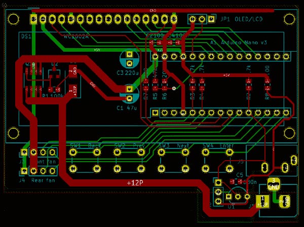
PCB Design
Designing is the basic and compulsory step for any PCB manufacturing. First the designer makes the blue print of the PCB as per the requirement. The most common software used for PCB designing is Extended Gerber also known as RS274X.
For the PCB designing, the Extended Gerber software has many pros as it encodes all the data required by the designer such as number of solder mask needed, number of copper layers, components. After the completion of the blueprint, it is encoded by Gerber Extended software. All the parts and other factors are verified and make sure for no errors.
After the confirmation by designer, the design is sent to the fabrication department. Before the fabrication, the design is verified again by the fabricator. This ensures the quality of final product.
Checking the Design
Next step is checking the design before printing. Here the engineer verifies as well inspect every part of PCB and search for and search for any malfunction component or faulty structure. After getting the confirmation from the engineer, the design moves to Printing.


