The Manufacturing Process
The PCB manufacturing process consists of complex processes which assures the better performance of the final product. The PCBs are divided into single, double or multilayer, the manufacturing process are same for first layer only. As there are various types of PCBs, some of them require more than 20 steps of manufacturing.
The steps required for the PCB manufacturing is depend on the complexity of the design. If any step is skip or ignore can seriously affect the performance of the PCB.
Parts of the PCB
Substrate is the most significant part of PCB, generally made of fiberglass. The fiberglass provides strength to the PCB and resistant to wear and tear.
It is depending on the board types; the copper layer can be copper foil or entirely coated by copper. No matter how much copper is used, the purpose remains the same of carrying the electrical signals to and from the PCB.
The solder mask is one the important part of the PCB as it protects the copper layer from short circuit and other environment factors.
It is the final part of the printed circuit board. It is usually on the component side which shows information such as symbols switch setting, part numbers, test points, and logos.
How PCBs are Made?
There are various steps in printed circuit board manufacturing. There are continuous observation required during the PCB manufacturing. Many of steps are completed by computer guided tools driven by machines. Testing is very crucial in PCB manufacturing as it ensures the superior quality of product and compulsory done before delivery.
The manufacturing of Printed Circuit Board starts with,
Step 1: Designing
Designing is the basic and compulsory step for any PCB manufacturing. First the designer makes the blue print of the PCB as per the requirement. The most common software used for PCB designing is Extended Gerber also known as IX274X.
For the PCB designing, the Extended Gerber software has many pros as it encodes all the data required by the designer such as number of solder mask needed, number of copper layers, components. After the completion of the blueprint, it is encoded by Gerber Extended software. All the parts and other factors are verified and make sure for no errors.
After the confirmation by designer, the design is sent to the fabrication department. Before the fabrication, the design is verified again by the fabricator. This ensures the quality of final product.
Step 2: Checking the Design
Next step is checking the design before printing. Here the engineer verifies as well inspect every part of PCB and search for and search for any malfunction component or faulty structure. After getting the confirmation from the engineer, the design moves to Printing.
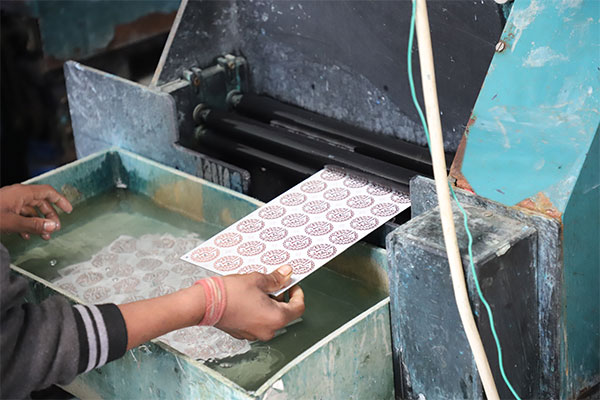
Step 3: PCB Design Printing
After the completion of checks, the PCB arrives in printing division. The PCB printing is different from the printing on paper. It is the different from the normal printer known as plotter printer. This makes a film of PCB which is transparent and you can say a photo negative of the board.
The PCB layers are in two colors.
Black Ink, Clear Ink.
The black ink is used for copper traces. The clear ink specifies the non-conductive areas of PCB like the base.
For the outer layers, this is opposite. The clear ink is for the line of copper pathways and black ink indicate the area the copper will be removed.
In the printing, each PCB layer and its solder a need separate film. For example, a two-layer PCB needs four sheets, one for layer and other for solder mask.
After printing, all the sheets are lined up and a hole is made known as registration hole. It is used as a guide to align the films in next process.
Step 4: Copper Printing for Interior Layers
In this step, the PCB manufacturing begins. After the printing of PCB design on laminated material, and copper is bonded on the same laminated piece. And this, works as a structure PCB. In the next process, copper is etched and revealing the blueprint.
Now this laminate panel is covered by phot-sensitive film known as resist. This resist is basically a photo-reactive chemicals which harden after exposed to UV light. This resist helps to technician for getting the exact match for blueprint and printed on photoresist.
After the alignment of resist and laminate through guided holes, get a UV blast. This UV light is pass through translucent parts of film which harden the photoresist and illustrate the portion where made the copper pathways. On the other side, the black ink does not allowed light to passed through it. So, that part is not harden and can be removed later.
After this, the board is washed by alkaline which removes the remaining photoresists. Then this board is pressure-washed which clean the surface thoroughly.
After drying process, the PCB has copper left on the surface. Then the technician verifies the PCB for any errors. If there is no error, it sends for next process.
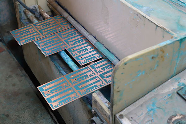
Step 5: Inner Layer Etching or Copper Removing
After these processes the inner layer of printed circuit board has an extra copper which have to be removed before fabrication process. The etching process covers the required copper on board and exposed the rest board to the chemical. This chemical etching process eliminate all unprotected copper from board and only PCB’s required copper left.
This process depends on the how much copper solvent is used for it. The small size has less copper where large PCB uses more copper which required more solvent to remove copper.
Step 6: Alignment of Layer
After the cleaning of PCB layers, they are sent for the layer alignment and gone through optical inspection. The inner and outer layers are aligned by holes which are punched before. For this, technician place all the layers in the optical punch machine. This machine drives a pin through holes to arrange layers of PCB.
Step 7: Optical Inspection
After that, the board pass through optical inspection and ensures for no defects. This optical inspection is very significant as once the layers are paced with any error cannot be reversed. For no defects, the Automated Optical Inspection or AOI compare the PCB with the Extended Gerber Design.
The Automated Optical Inspection is very important and without it, there are chances if short circuits, not effective and the extra copper remaining in etching process stays there. This inspection blocks the defective boards from going to next process. The AOI is also repeated for the outer layers to inspect imaging and etching.
After these inspections, PCB sent for the next manufacturing process.
Step 8: PCB Layer Laminating
At this station all the PCB layers are place together and ready for lamination. After the finalizing of the layers the lamination process begins. There are two steps in laminating. One is lay-up and laminating.
The outer of PCB is made of fiberglass which have been soaked or pre-coated with epoxy resin. The substrate is also covered in layer of thin copper foil and it contains etching of copper. The outer and inner layers are put together by metal clamps on press table. These layers are bind through specialized pin. The process starts by placing layer of pre-coated epoxy resin. After that a layer of substrate and copper foil are placed above the resin. This is finished with the copper sheet.
After that it is ready to be pressed. Then these layers are taken to the mechanical press and pressed. In this process, the pins are punched in stack of layers.
When the layers are fixed properly, the PCBs are taken to the laminating press. There are heated plates in the laminating press which apply heat and pressure for stacking of layer. This heat melts the epoxy and pressure presses the stack of layers.
Step 9: Drilling
The X-ray machine is used to locate drill spots before drilling. Then the guided holes are drilled for the PCB stacking and secured the PCB. For drilling, a computer-operated drill is used to make holes according to Extended Gerber design. Once the drilling is over, the leftover copper at the edges is filed off.
Step 10: PCB Plating
After drilling, the plate is ready for the plating. The chemical is used to bind the different layers of the PCB together. After cleaning, the PCB is washed through various chemicals. In bathing, the panel is coated with micro layer of copper to outer layer and also fill the holes. This bathing coats the walls of previously drilled holes.
Step 11: Outer Layer Imaging
In the beginning, a photoresist was applied on the PCB. In this step, another layer of photoresist is applied. Here the photoresist is only applied to outside layer and it needs to be imaged. After the photoresist coating and imaging, plated same as the inner layers. There is a difference in this process. In this process, the outer layer get tin plating in order to help the outside layer.
Step 12: Outer Layer Etching
In the outer layer etching, the tin protects the copper during the etching process. Extra copper is removed by the solvent and tin protected copper remains.
The major difference between inner and outer layer etching is the removed area. Here the dark ink is used for the conductive area and the clear ink is used for the non-conductive area. For the outer area, this process is reversed. The non-conductive layers are covered in dark ink and copper is covered in light ink. The light ink is for tin plating which covers the copper and also protect it.
Step 13: Outer Layer AOI
Same as the inner layer, the outer layer also undergone the AOI or Automated Optical Inspection. This inspection ensures that the layers have been met the design requirements. And it also assures that previous processes removed extra copper and ensure proper functioning of PCB with proper electrical connections.
Step 14: Solder Mask Application
The boards need thoroughly cleaning before applying solder mask. After cleaning, board’s surface is covered with solder mask and ink epoxy. Then, ultraviolet light indicates the area where the solder mask needs to removed.
After removing, the PCB enters into oven to curing the mask. The solder mask protects the copper of board from external damaging by oxidation and corrosion.
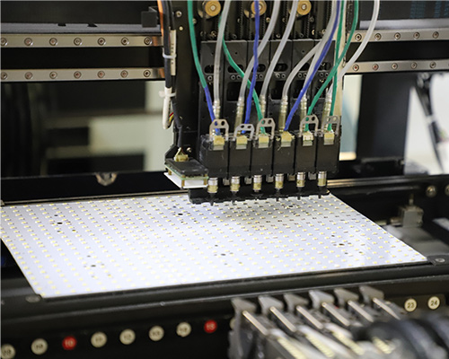
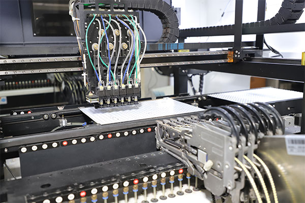
Step 15: Application of Silkscreen
The PCB needs to display information on the surface of it. This printing is known as silkscreen application or legend printing.
This information contains of:
- Manufacturer Mark or Logo
- Part Number
- Pin Locator
- Warnings
- Others
The above information is printed with inkjet printer.
Step 16: Finishing
The PCB coating with various conductive materials. There are various materials used for the coating.
Immersion Silver: Low signal loss, lead-free, RoHS compliant, finishing with oxidize and tarnish.
Hard Gold: Durable, long shelf life, RoHS compliant, lead-free, expensive.
Electroless nickel immersion gold: Provide most common finish, long shelf life, RoHS compliant, expensive than other options.
Hot air solder leveling (HASL): cost-effective, lead-free, contains lead, no RoHS compile.
Lead-free HASL: cost-effective, lead-free, RoHS compliant, reworkable.
Immersion tin: suitable for press-fit applications, high tolerance for holes, RoHS compliant, Soldering Problems.
Organic solderability preservative: RoHS compliant, cost-effective, short shelf life.
Electroless nickel electroless palladium immersion gold (ENEPIG): Maximum solder strength, less corrosion, less cost-effective.
The selection of plating materials is depending on the design and budget. This allows technician to mount electronic components. This coating also covers the copper and prevent oxidation.
Step 17: Reliability Test
After the finishing, the PCB goes through series of tests on different parts of the PCB to ensure 100% functionality. This PCB must reach the IPC-9252 standards. The purpose of these tests is to check continuity and isolation tests. The continuity test finds any disconnections in PCB refers as ‘opens’. And the isolation test checks the isolation value of various parts of the PCB for any shorts. Also, other tests are performed to functionality of the PCB. The next test is “bed of nails” test. In this test, multiple springs are attached to the various points of the PCB. These points apply up to 200 grams of pressure check how long the PCB withstand with the pressure.
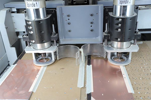
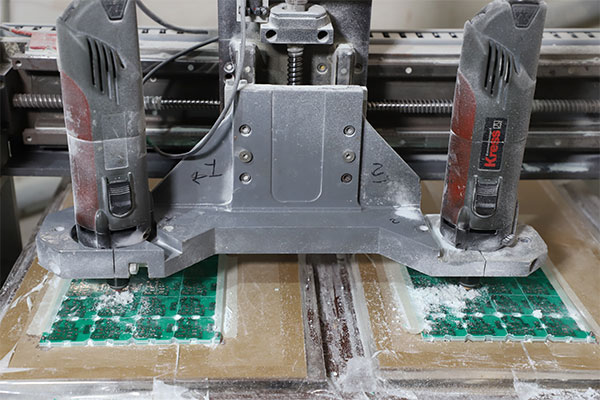
Step 18: Profiling and Routing
The profiling is required for the technician to recognize the size and shape of particular PCB to cut from the main board. This information can be found from the Gerber files.
The routing out also called scoring, easily separates the boards. Here the CNC machine, make small pieces with the edges. And this edge allows the board to break off without spoilage.
Step 19: Visual Inspection & Quality Check
After breaking apart, the PCB must pass through inspection before packaging and shipping. This checks also verifies other standards such as:
- Hole sizes must be same for all layers according to design.
- The board size must be as per the design.
- Technician must take care that dust should away from the board.
- The finished products must not have any sharp edges or burrs.
- Boards which fail the electrical reliability tests, send for the repair and retesting.
Step 20: Packaging & Delivery
Packaging & Delivery is the last stage of the PCB manufacturing. The packaging materials seals the boards and protect it from the dust and other damaging materials.